Many of our customers look to us to help them with their flatness measurement projects. Sometimes they are looking to validate their substrate materials before they spend the money populating the substrates with their products and devices. Other times they are looking to validate the flatness or coplanarity of a finished part surface to see if it conforms with the design tolerances they initially laid out.
When surfaces are large, say greater than 250mm or 10″ in size, measuring flatness down to the micron level becomes more challenging. This is because the motion process (scanning of the sensor) contributes error to the measurement result. Selecting the right measurement sensor and motion control equipment is important. Let’s walk through the things to think about for micron level flatness measurements.
Selecting the right measurement device for micron level results
If you are trying to resolve measurements in the micrometer realm, you will need to select a sensor with enough resolution to “see” that values you are trying to achieve. This means that you need a sub-micron resolution sensor in order to measure to single micrometer tolerances. Typically, we suggest that a 10:1 ratio between measurement resolution to measurement tolerance be used. If your tolerance is +/-3um of flatness, your sensor should be at least capable of seeing changes in height down to 300 nanometers.
The sensor also needs to be selected based on the surface properties you are trying to measure. If the surface is reflective or transparent certain sensors are better than others. Similarly, if you require a dense amount of data collected on each surface there are sensors that act as an “array” to collect more data quickly. Finally, depending on the texture of your surface the point size or shape that the sensor uses for measurement becomes important. Smooth surfaces are more forgiving and allow for a wider selection of sensors to be used.
Below we are showing the roughness of a piece of glass. This piece looks and feels very different at a microscopic level. When viewing it by eye, you cannot see anything other than a perfectly flat surface. However, under a microscope that all changes.
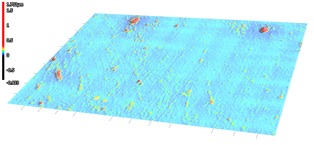
The glass surface above was imaged by a confocal microscopic. Not all surfaces will be this flat, and some will appear smoother.
Choosing the right scanning system for your needs
Once the sensor technology is chosen an equally important decision is waiting. The positioning (or scanning) system is critical to the precision of the results that you will get from the scanning process. If the positioning system produces errors while it is moving the sensor over the surface. Your measurement result will also have those errors imbedded in them.
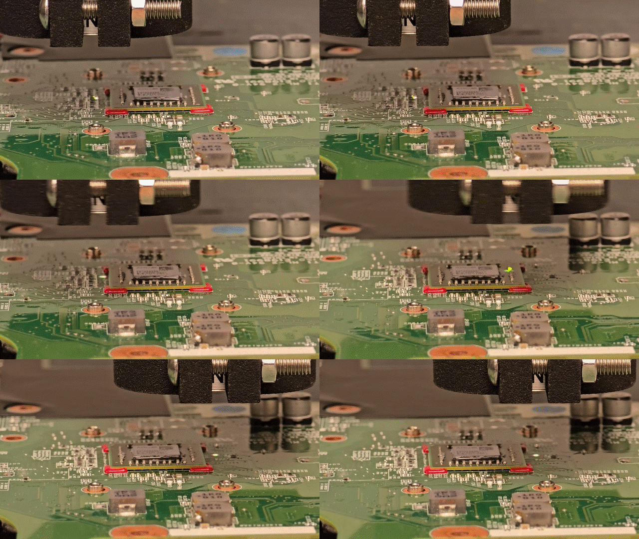
Showing a scanning process using a point sensor. Here, we are scanning a chip mounted to a board.
The error motions of the positioning system need to be accounted for in your tolerance budget for the measurement. In the example above, we talked about a 300nm tolerance for the measurement sensor. What was yet to be accounted for was the positional accuracy and repeatability of the scanning equipment. If the tolerance is +/-3 micrometers, you’ll need to set aside some error budget for the scanning motion equipment. In this case, we suggest maintaining a 10:1 ratio if possible. But sometimes the economics don’t work out the way we want them to. In order to maintain this ratio and achieve a measurement repeatability of +/-300 nanometers we would often need to deploy equipment like air bearing stages and high grade granite reference surfaces. This increases the cost of the equipment, but gives you a much better chance of hitting these tight tolerances.
Let’s demonstrate what is possible with a more economical scanning solution.
Application example: glass sheet measurement
For this example, we are mearing a glass sheet by collecting profile data. We’re using a sub-micrometer resolution point sensor. We’re also using a precision motion stage, albeit a mechanical bearing stage. Finally, we are going to use the sensor to calibrate any repeatable flatness errors that the stage and workpiece holding surface have in them.
Below is the scanning process in real time. As you can see the sensor is moved rapidly over the surface of the glass. The sensor is turned on and off while we are collecting data.
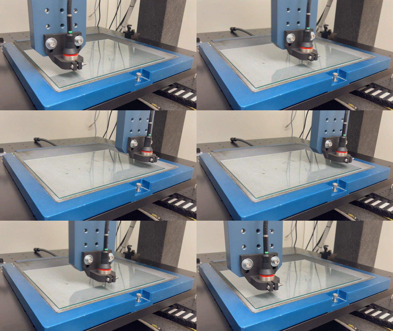
After the scanning process we are left with a dataset of height values from the sensor. These datapoints are collected and aggregated by Peak Metrology’s software. Then, we analyze them using a topography package. For this example, we will be looking at individual profile scans and plotting them in 2D for visualization.
We need to take out the form of the vacuum chuck holding the glass surface. This will help us expose the true flatness variation across the glass substrate. When we take out the form of the chuck we are left with the flatness profile of the glass surface itself. See the plots below showing the flatness data before the form is removed, the form we are removing, and the data after the form is removed.

Above: Plot showing the measurement data retrieved from the sensor while scanning the length of the substrate surface. Notice the slope in the data.

Above: Plot showing the measurement data retrieved from supporting surface under the glass. Note how it matches the form of the measurement data from the glass above.
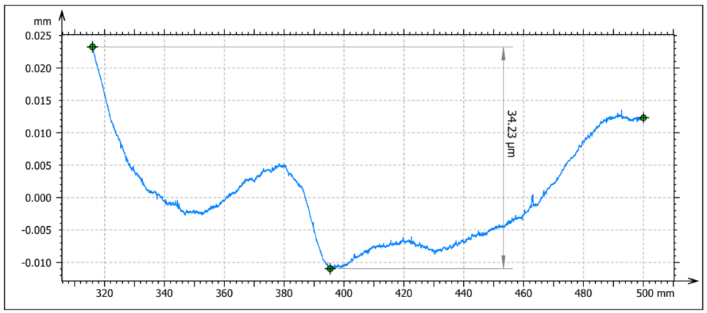
Above: When subtracting the slope of the supporting surface from the dataset with the glass included we are left with this result. This result shows only the flatness profile of the glass itself.
We then repeated the scanning process 10 times. We used the same form measurement scan from the supporting chuck’s surface on all 10 datasets. What we are left with is the peak to valley flatness measurement values of the substrate itself.
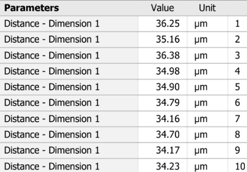
The peak to peak range between the measurements is 2.2 micrometers. This is how repeatable the system is at making flatness measurements on this surface.
Application example: Flat Optical Surface Measurement – Understanding Scan Repeatability
In this example, we are measuring flatness over an XY area, and using an optical flat to verify the flatness uncertainty of the measurement process.
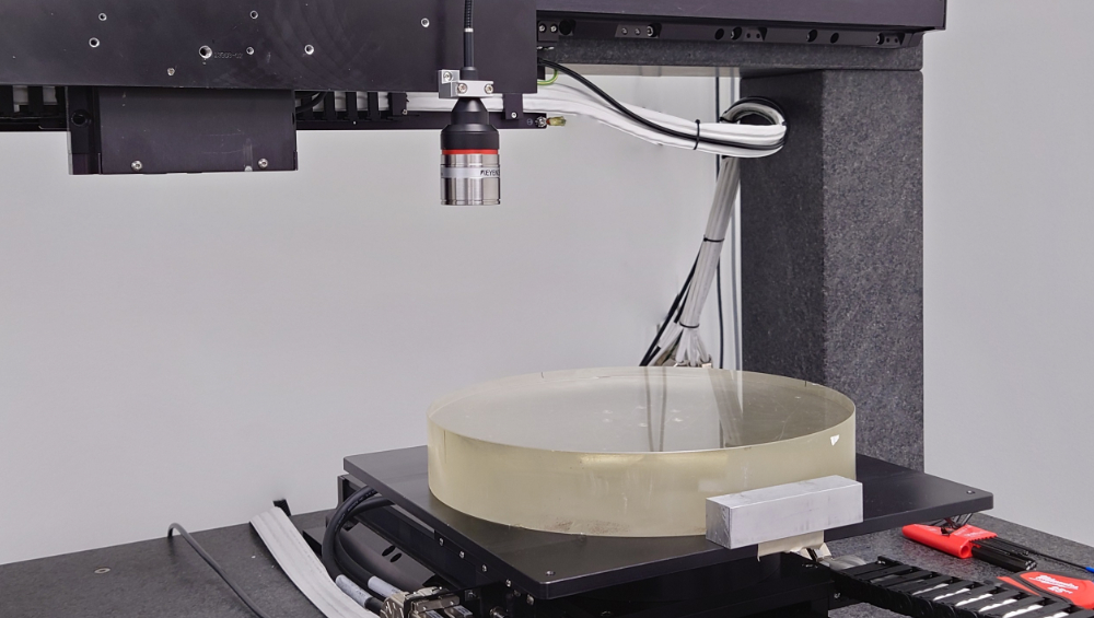
Showing a 300mm diameter precision optical flat. The optic moves on a stage in the Y direction and the sensor moves on a stage in the X direction. We used both stages to scan the optic in the XY plane to retrieve Z height values from the confocal point sensor.
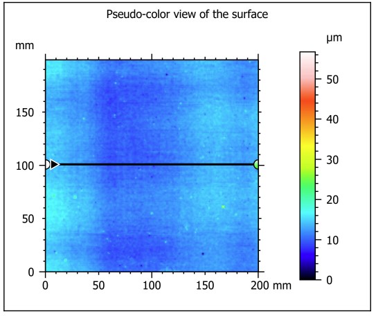
Showing the Z height values measured by the sensor over a 200mm area. This data was taken 10 consecutive times to produce a repeatability dataset that we can use to determine the uncertainty of the measurement.

Showing a 200mm profile of all 10 datasets plotted against each other. The dispersion between the lines (shown max in red) demonstrates that there is some uncertainty in the measurement due to various factors.
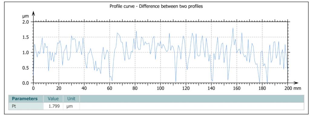
Showing the peak to peak difference between the 10 different measurement runs. This shows that when we measure the optic 10 different times, the profile flatness results vary by 1.8um worst case. This is the repeatability limitation of the setup and scanning process that was implemented for this application.
conclusion
The lesson here is that with this sensor and this scanning stage setup we are able to achieve a ~2 micrometer flatness measurement repeatability. There are solutions that will achieve a tighter tolerance than this. We provide these solutions as well.
It’s important to consider both the sensor selection and positioning system selection with respect to the flatness tolerances you need to inspect.
For more guidance and consultation please reach out to us. We offer full engineering and laboratory testing services to help guide our customers towards the right solution to their measurement challenge.